Utah Nanofab
The Utah Nanofab brings together two teams of experienced researchers, engineers and scientists with backgrounds in nano-fabrication, nano-scale surface analysis, and industrial process design.
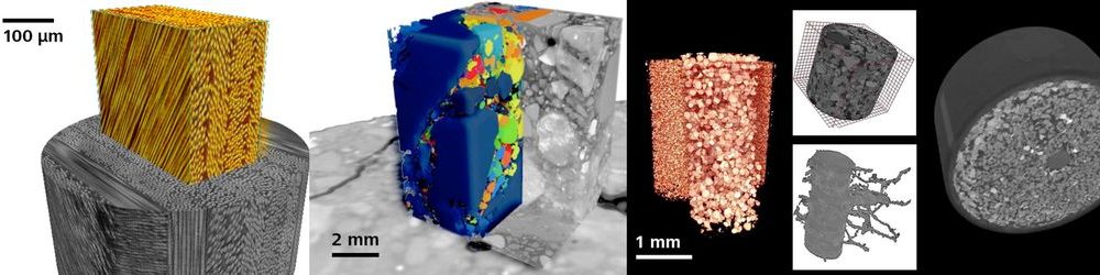
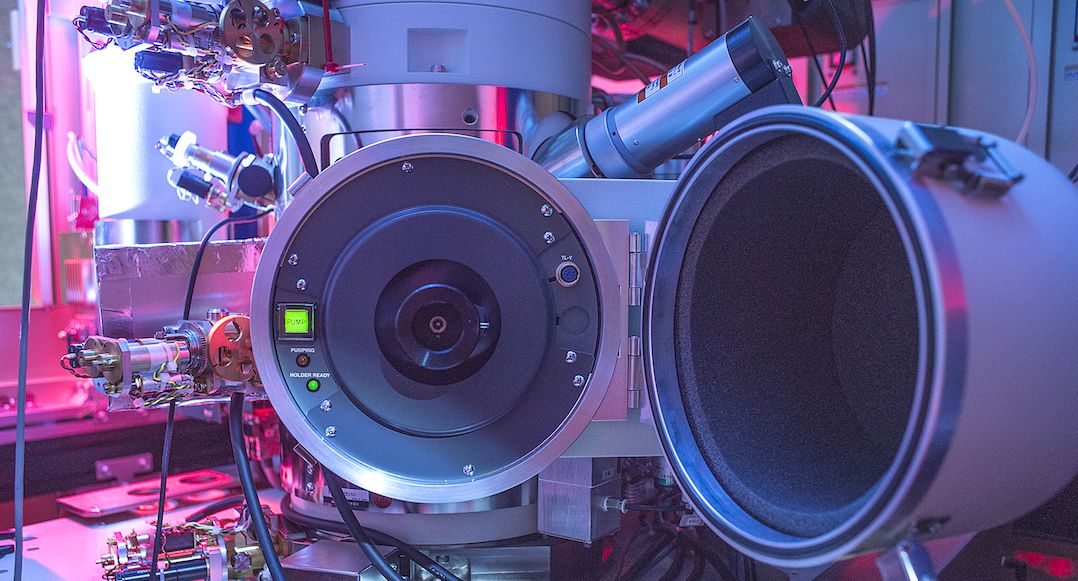
Electron Microscopy & Surface Analysis Lab
The Electron Microscopy & Surface Analysis Lab is the Utah Nanofab’s analysis branch. It is home to the ~5,000 square foot microscopy suite containing optical, electron, and ion microscopes. The lab’s team of scientists and researchers have years of experience in the fields of surface topography, surface chemistry and optical and dielectric properties of materials. Find out more about specific instruments and techniques at the Surface Analysis Lab’s website or contact us to find out what we can do for you.
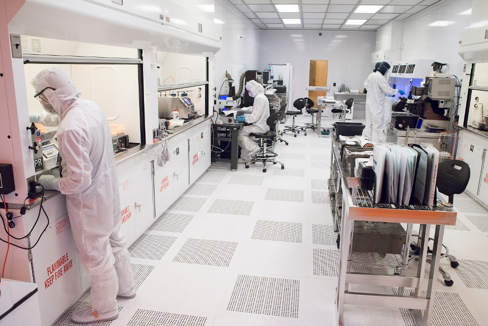
Utah Nanofab Cleanroom
The Utah Nanofab Cleanroom is the Utah Nanofab’s fabrication and process design branch. We have a team of experts with years of industrial and academic experience in nano-fabrication techniques. Our class 100/1000/10,000 cleanroom provides world-class equipment for lithography, deposition, etching, packaging, micro 3D printing, laser patterning, and more. We would be happy to talk with you and your organization about how we can provide access to the tools or experts you need to engineer successful and reliable fabrication processes. Please browse our processes page or contact our staff to find out more.
Sponsors