How to Have Your Substrates Diced/Singulated
- Contact Nanofab Cleanroom staff with dicing details (material, substrate size, chip dimensions) https://www.nanofab.utah.edu/lab-staff/#process (Brian Baker)
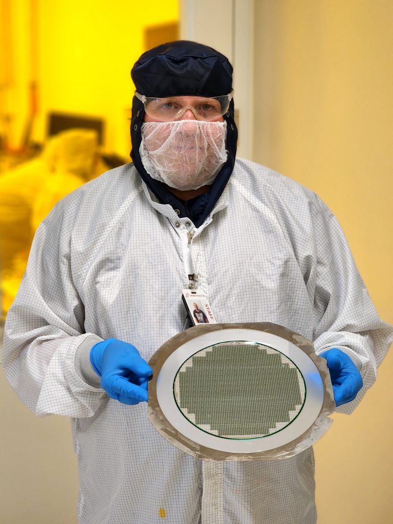
- Substrate sizes diced: Small pieces up to 200mm wafers.
- Materials diced: silicon, glass, fused silica, sapphire, gallium oxide, and more.
- Staff will examine your file and give you an estimate for print time and cost
- Set up a Nanofab account (https://workauth.cores.utah.edu/#/offcampus)
- Ship your substrates to Nanofab Cleanroom staff
- After you approve/authorize the design, staff will print and ship your photomask or patterned substrate to you
How to Have Your Wafers Anodically Bonded
- Contact Nanofab Cleanroom staff with bonding details and requirements https://www.nanofab.utah.edu/lab-staff/#process (Brian Baker)
- Substrate sizes bonded: Small pieces up to 4″ wafers
- Materials bonded: silicon to borosilicate glass
- Staff will give you an estimate for print time and cost
- Set up a Nanofab account (https://workauth.cores.utah.edu/#/offcampus)
- Ship your substrates to Nanofab Cleanroom staff
- After you approve/authorize the process, staff will bond your wafers and ship them back to you