|
Image
|
Title | Authors | Links | Nanofab Process used |
|---|---|---|---|---|
 |
A facile dry-PMMA transfer process for electron-beam lithography on non-flat substrates | Jong-Hyun Kim, etc | https://ieeexplore.ieee.org | Electron Beam Lithography |
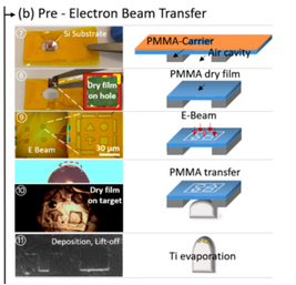 |
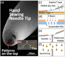
A Facile Dry-PMMA Transfer Process for Electron-Beam Lithography on Non-Flat Substrates | Jong-Hyun Kim Qin Zhou Jiyoung Chang |
https://ieeexplore.ieee.org | Lithography |
 |
Optical patterning of features with spacing below the far-field diffraction limit using absorbance modulation |
Farhana Masid Trisha L. Andrew Rajesh Menon |
https://www.osapublishing.org | Lithography |
 |
MICROFABRICATION OF NANOPORE DEVICES WITHOUT NANOLITHOGRAPHY | L. Chen1 , Y. Wang1 , and C.H. Mastrangelo1 | https://ieeexplore.ieee.org | CVD ALD Lithography |
 |
Surface analysis of photolithographic patterns
using ToF-SIMS and PCA
|
Manish Dubey Kazunori Emoto Fang Cheng Lara J. Gamble Hironobu Takahashi David W. Grainger David G. Castner |
https://onlinelibrary.wiley.com | Deposition Lithography Dry Etching |
 |
Quartz Nanopore Membranes for Suspended Bilayer Ion Channel Recordings |
Anna E. P Schibel Thomas Edwards Ryuji Kawano. Wenjie Lan, Henry S. White |
https://pubs.acs.org | Etching |