|
Image
|
Title | Authors | Links | Nanofab Process used |
|---|---|---|---|---|
 |
Bi-layer encapsulation of utah array based nerual interfaces by atomic layer deposited Al2O3 and parylene C | Xianzong Xie | https://ieeexplore.ieee.org | Al2O3 deposition |
 |
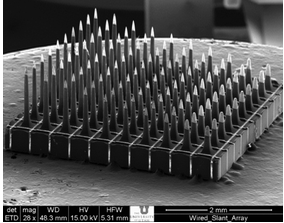
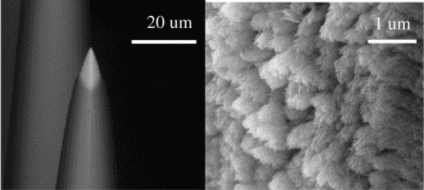
Long term performance of porous platinum coated neural electrodes | M. Leber1 & R. Bhandari1,2 J. Mize3 D. J. Warren3 M. M. H. Shandhi1 F. Solzbacher1 S. Negi1,2 |
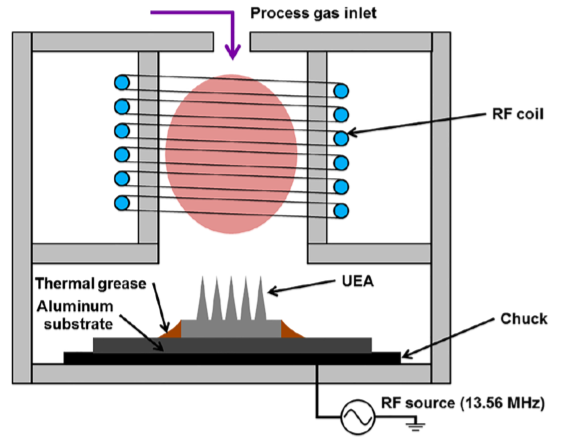
https://link.springer.com | Oxford Plasmalab System 100 |
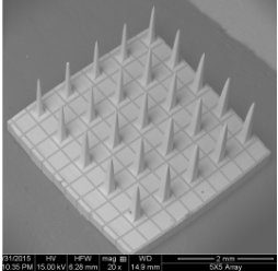 |
A Novel Method of Fabricating High Channel Density Neural array For Large Neuronal Mapping | M.M.H. Shandhi1 M. Leber1 A. Hogan2 R. Bhandari2 and S. Negi1 |
https://ieeexplore.ieee.org |
Chemical Vapor Deposition// SEM |
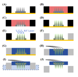 |
Novel Method of Fabricating Self-Dissolvable and Freely Floating neural Array | M. Leber R. Bhandari F. Solzbacher S. Negi |
https://ieeexplore.ieee.org | Lithography,Oxford Plasmalab 80 Plus, Wet etching |
 |
Maskless method to selectively etch Parylene-C from high aspect ratio neural devices | M. Leber M. M. H. ShandhiR. Bhandari ; S. Negi |
https://ieeexplore-ieee-org | PlasmalabSystem100 |
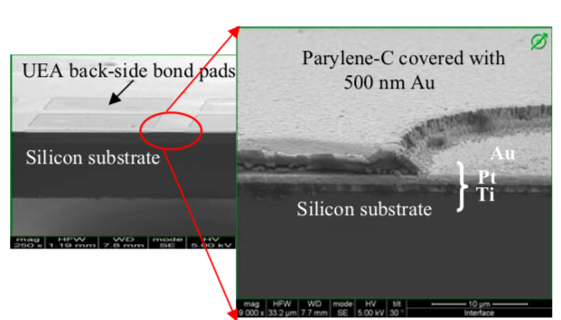 |
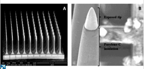
Parylene C-based flexible interface for neuroprosthetic applications | Rajmohan Bhandari Sandeep Negi R. Van Wagenen Florian Solzbacher |
https://ieeexplore.ieee.org | Sputtering Dry Etching CVD |
 |
Factors affecting degradation of sputtered iridium oxide used for neuroprosthetic applications | Sandeep Negi Rajmohan Bhandari Rick Van Wagenen Florian Solzbacher |
https://ieeexplore-ieee-org | Sputtering |